
东莞市玮孚电路科技有限公司专注电路板制造,打造一流PCB企业
全国咨询热线:13712727627
用精湛的技术制作中国世界品牌
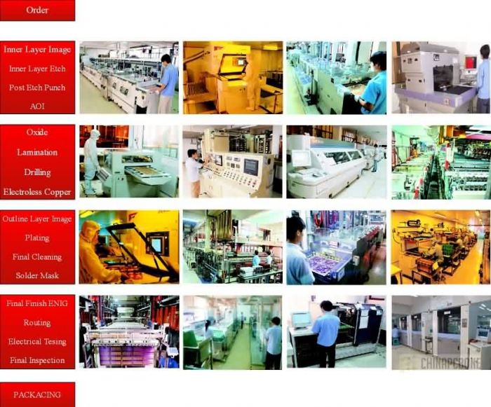
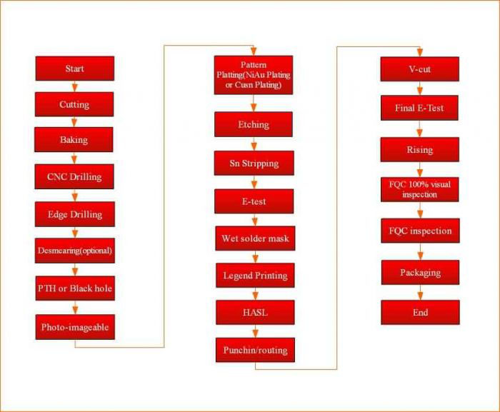
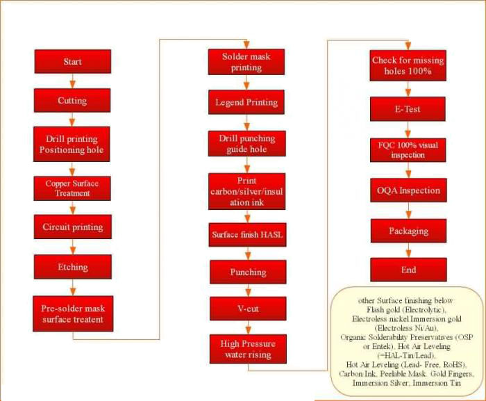
Every year, VIAFINE have to put in a lot of manpower and money to continuously upgrade Manufacturing Processes to meet customer newer and higher technical requirements and lower costs.
Our processes are transparent to customers. You can see an outline of each step on Manufacturing PCBs below.
Standard Default Criteria for PCBs material and Processing:
| 1. | IPC Standard | Inspection and test criteria will be based upon IPC-A-600 and IPC-6012, Class 2 unless otherwise specified on customer drawings or specifications. |
| 2. | Markings | Customers can specify the Marking. default marking is VIAFINE branch factory's marking. |
| 3. | Laminate | Single side boards: FR-1, FR-2 or FR-4 glass epoxy laminate per IPC-41011 with a minimum Tg 110 C. Starting clad copper weight to be 1?OZ / FT 2 minimum. Double sided plated-through boards: King Baord, FR-4 glass epoxy laminate per IPC-4101 with a minimum Tg of 130 C. Starting clad copper weight to be 0.5?OZ / FT 2 minimum. Multilayer boards: King Board, FR-4 copper-clad glass-epoxy? ( tine core ) and laminateand material ( prepreg ) per IPC-4101with a minimum Tg of 135 C Starting clad copper weight to be 1 OZ / FT 2 minimum on all internal layers and 0.5 OZ / FT 2 minimum on external layers. |
| 4. | Copper Plating | Holes with copper pads on both sides are to be copper plated through. Copper plating thickness will be in accorde with IPC-6012, Class 2 (0.0008" avg. minimum thickness ). When copper pads on artwork are smaller or the same size as the corresponding finished holes, SCT will regard the hole as not requiring plating. |
| 5. | HASL | Copper features exposed by PCB Solder Mask, except nickel / gold plated edge contacts, will be coated by Hot Air Solder Leveling (HASL). SCT monitors the HASL processes to ensure that boards meet the solderability requirements of IPC6012 class 2. |
| 6. | Nickel/gold Plated surfaces | Nickel/gold plated surfaces: For contact surfaces: a minimum thickness of 0.8 gold over 150 nickel; and for solderable surfaces. |
| 7. | Holes Dimensional | Finished plated through hole size tolerances will be in accordance with IPC-D-300, Class 2: Finished holes up to 0.032" ... 0.003" Finished holes from 0.033" to 0.063" ... 0.004" Finished holes from 0.064" and larger ... 0.006". |
| 8. | Board Size | Max. Board Size 864 x 610 mm (34" x 24") |
| 9. | Soldermask | Green Liquid Photo Imageable Solder Mask (LPI) will be applied over bare copper traces. The mask material will comply with IPC-SM-840 Type B, Class II. Unless specifically prohibited by the customer. |
| 10. | Comp. Mark | When required, nomenclature will be printed on the component side of the board with white non-conductive epoxy ink or acrylate equivalent. |
| 11. | Bow and twist | Bow and twist will not exceed 0.75% for boards bearing surface SMT mount components, and 1.5% for all other boards. |
| 12. | Others | Unless otherwise specified, thickness tolerances will be 10% of the finished board thickness, not including surface copper. |

TEL:0769-87086168 MOB:13712727627 EMAIL:sales@viafine.com
总公司地址:广东省东莞市沙田镇环保南路13号4号楼505室
版权所有:Copyright © 东莞市玮孚电路科技有限公司 粤ICP备XXX号-1
Powered by 赢网科技